Application note ·
From 2D AXI to inline 3D planar CT: inspecting 20-layer HDI boards and back-drilled vias in production
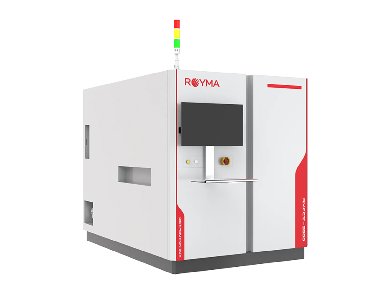
The RMPCT5500 planar computed tomography (CT) machine from Royma Industrial CT brings 3D inspection of multilayer and HDI boards onto the production line. It reconstructs more than 300 slices per scan at up to 2 s per field of view. Back-drilled vias, BGA joints and through-hole fill are measured at the layer where they sit.
The machine is built for quality managers and test engineers in PCB and PCBA production. It runs inline or at-line, takes boards up to 760 × 660 mm and 1–7 mm thick, and reports to the plant’s MES. You get a measured result per via and per joint instead of a flattened image to interpret.
Planar CT separates the layers that 2D AXI superimposes
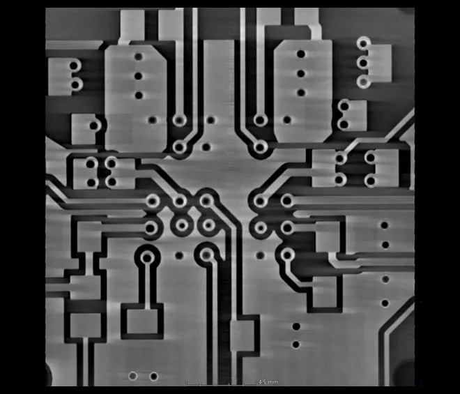
A 2D automated X-ray inspection (AXI) image projects the whole board into one picture. On a board with 20 or more layers, vias, copper planes and BGA balls on both sides overlap in that picture. A void in one joint and a harmless overlap with a component below can look the same.
Back-drilled vias show this limit most clearly. A 2D image shows that a via has been drilled. It does not show how long the remaining stub is or how much copper is left in the barrel, and those two values decide whether the via passes.
Multilayer and HDI board production for automotive power electronics is growing in Europe and Asia. As layer counts and via density rise, so does the number of joints that a single projection cannot resolve.
The RMPCT5500 reconstructs the board slice by slice
The RMPCT5500 uses planar CT, also called laminography, for flat parts too large for a rotating-sample scan. The X-ray source and detector move relative to the board instead of turning it, at a projection angle of 30° or 45°. From 32 up to 1024 projections, the machine reconstructs more than 300 slices in the XY, XZ and YZ directions.
Three imaging modes run on the same hardware: 2D, 2.5D and 3D planar CT. You can screen a board in 2D and switch to 3D for the joints that need it. Resolution is selectable between 3 and 30 µm to match via diameter and ball size.
The source runs from 40 to 180 kV and 10 to 300 µA. A 14-bit flat-panel detector with 2304 × 2940 pixels records up to 15 frames per second.
“A 2D image of a 20-layer board shows every layer at once,” says Gabor Szabo, Sales Director Europe at Royma Europe. “Planar CT gives your test engineers a slice at the depth where the defect actually is.”
Back-drill depth and solder joints are measured automatically
For back-drilled vias, AI-based measurement determines the remaining stub depth and the residual copper. The check runs without an operator reviewing every slice. A rejected board is flagged against the via that failed, not with a board-level result alone.
The same scan covers the solder joints. The software detects voids, open joints and missing solder, shorts and bridging, including BGA short circuits. It reports insufficient or excess solder, inadequate through-hole fill, misalignment, solder-ball shift, the pillow effect and lifted leads. Cracks, solder splatter and foreign matter appear in the same volume.
Components covered include BGA, CSP, QFN, QFP and SOP packages, chip components and power modules.
“The line gets a via number and a defect class, not just a rejected board,” Szabo adds. “That turns the CT station into a yield tool rather than a final gate.”
Automated handling, AOI and MES keep CT in the line
An optical camera first captures a navigation image, and the regions of interest are selected on it. Loading and unloading are automatic, and the scan starts with one click. A laser-measured reference plane compensates board warp of up to ±2 mm at component level, so the slices stay aligned to the joint layer.
Synchronous automated optical inspection (AOI) runs alongside the X-ray check. Results pass to the plant’s MES with the position and defect class of each finding. The same machine runs inline or at-line.
Boards weigh up to 3.5 kg as standard, with 5 kg or 8 kg as options. A pneumatic clamp holds the board by a 3 mm edge.
Resolution, field of view and inspection time depend on each other. Plan the configuration around your thickest board and your smallest via, and test it on your own boards before it is fixed.
| Stated figure | RMPCT5500 |
|---|---|
| Operation | Inline or at-line; synchronous AOI; MES connection |
| Imaging modes | 2D, 2.5D and 3D planar CT; more than 300 slices (XY, XZ, YZ) |
| Projection angle | 30° or 45° |
| Projections | 32 to 1024 |
| Inspection time | Up to 2 s per field of view |
| Resolution | Selectable, 3–30 µm |
| Field of view | Up to 57 × 73 mm, depending on resolution |
| X-ray source | 40–180 kV, 10–300 µA, up to 40 W target power |
| Detector | Flat panel, 2304 × 2940 pixels, 49.5 µm pixel size, 14-bit, up to 15 fps |
| Board size | Up to 760 × 660 mm, 1–7 mm thick, 3 mm clamping edge |
| Board weight | Up to 3.5 kg (optional 5 kg or 8 kg) |
| Warp compensation | ±2 mm, laser-measured reference plane |
| Back-drill analysis | AI measurement of stub depth and residual copper |
Royma Europe offers test scans of customer boards and assemblies on the RMPCT5500. Contact Gabor Szabo, Sales Director Europe, Royma Europe, gabor_szabo@roymatek.eu, +49 15156503316 – www.roymatek.eu. Further inspection tasks are described on the consumer electronics and automotive application pages.
Royma Europe, Leibniz Universität Hannover – Institut für Produktentwicklung und Gerätebau, Gebäude 8143, An d. Universität 1, 30823 Garbsen, Germany.