
Application note
Application notes.
One inspection task per note: the part, the method and what the data shows.
Application note ·
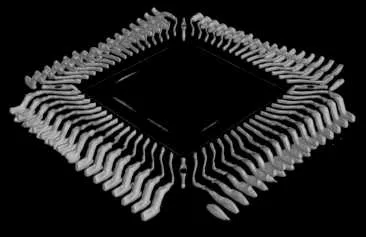
Royma RMPCT5500 brings inline planar CT to IC-substrate and advanced packaging lines
Application note ·
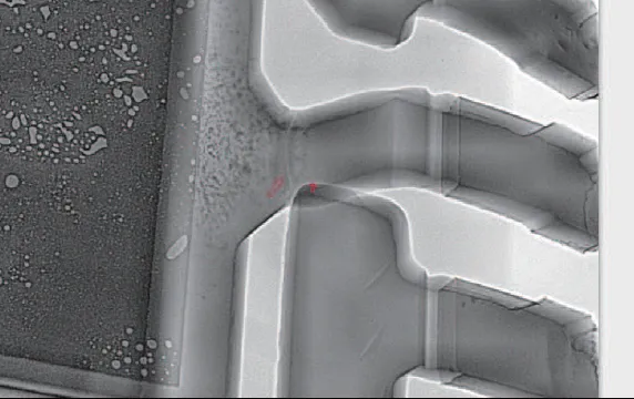
Royma RMCT2000HR brings sub-micron CT to hybrid bonding void inspection
Application note ·
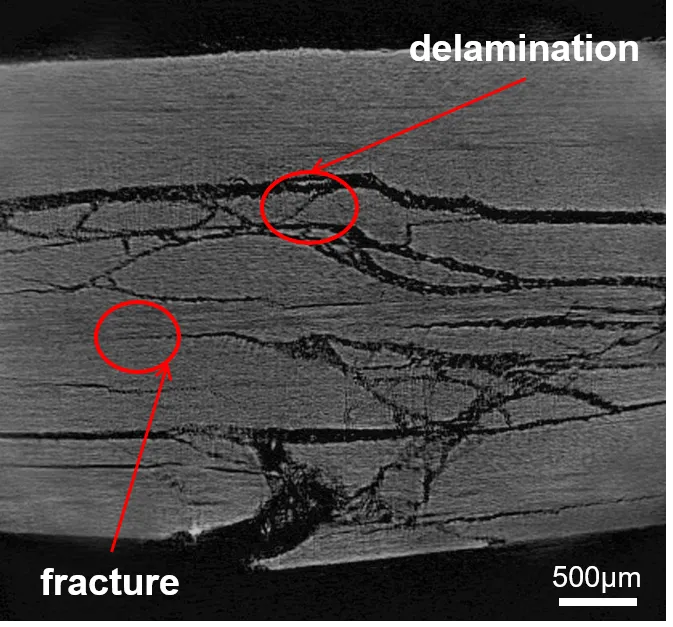
Royma CT inspection of launcher structures: welds, bond lines and composites
Application note ·
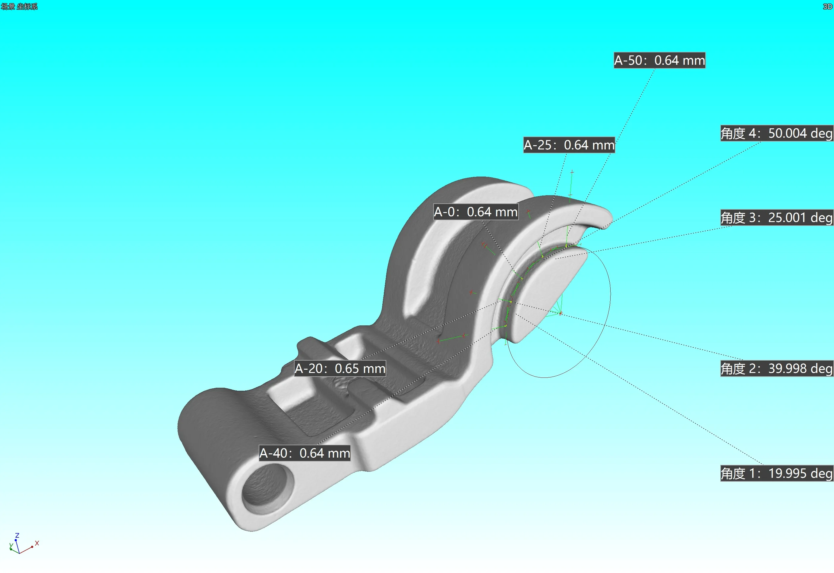
Royma RMCT4000 brings additive manufacturing CT for porosity and CAD checks to aerospace parts
Application note ·
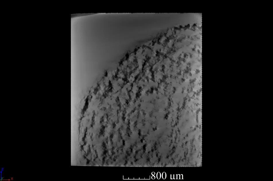
RMCT10000 delivers a CT scan of the entire sample for titanium additive-manufactured parts before machining
Application note ·
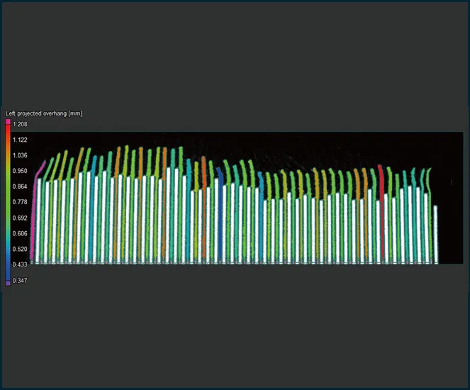
Why 2D X-ray misses prismatic-cell overhang faults – and what 100% inline 3D CT changes for LFP and ESS cell lines
Application note ·
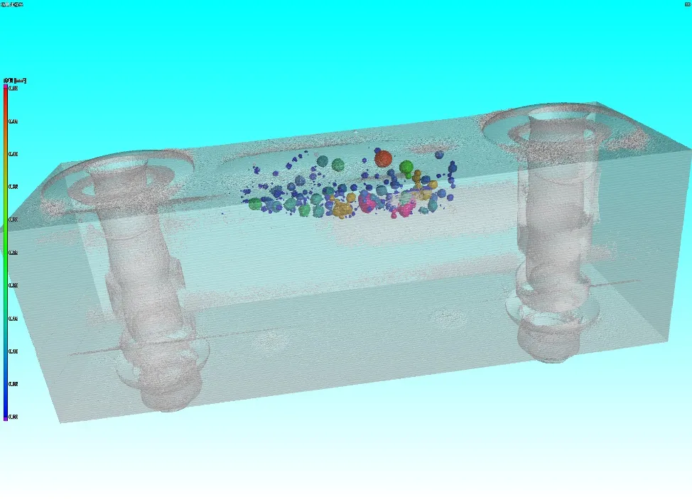
Proving porosity, core-shift and wall-thickness control as foundries move to printed sand cores
Application note ·
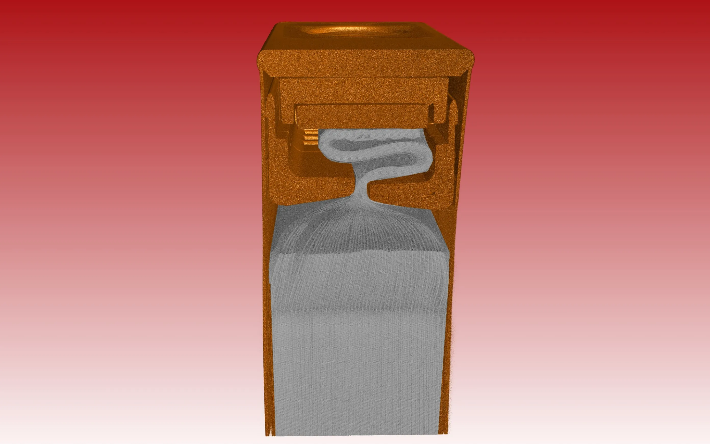
Beyond the electrode stack: CT of top-cover laser welds, safety valves and seal balls on prismatic cells
Application note ·
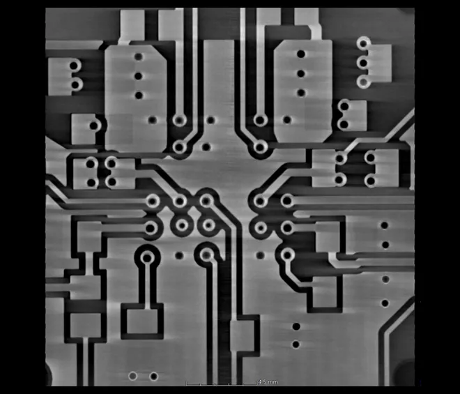
From 2D AXI to inline 3D planar CT: inspecting 20-layer HDI boards and back-drilled vias in production
Application note ·
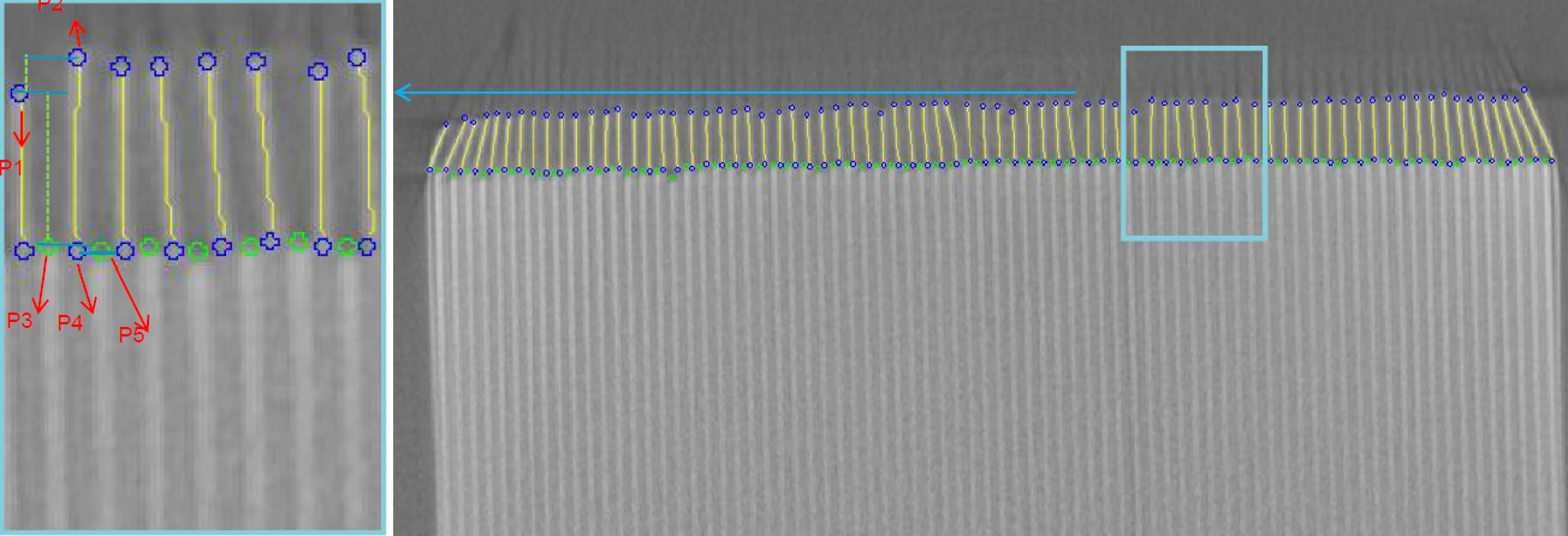
From sorting to fixing: how 100% inline cell CT feeds defect data back to the stacking line
Application note ·
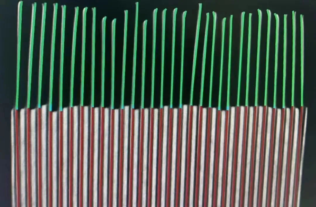
Forecasting the ROI of 100% inline cell CT: how to measure your own false-reject and escape rates before you buy
Application note ·
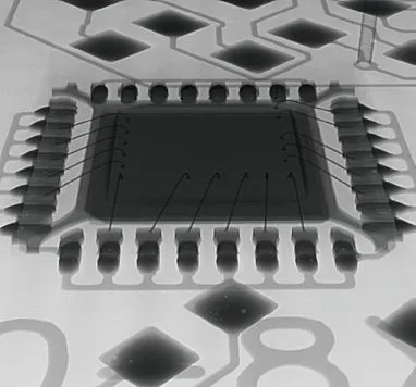
Seeing inside advanced semiconductor packages before they leave the lab
Application note ·
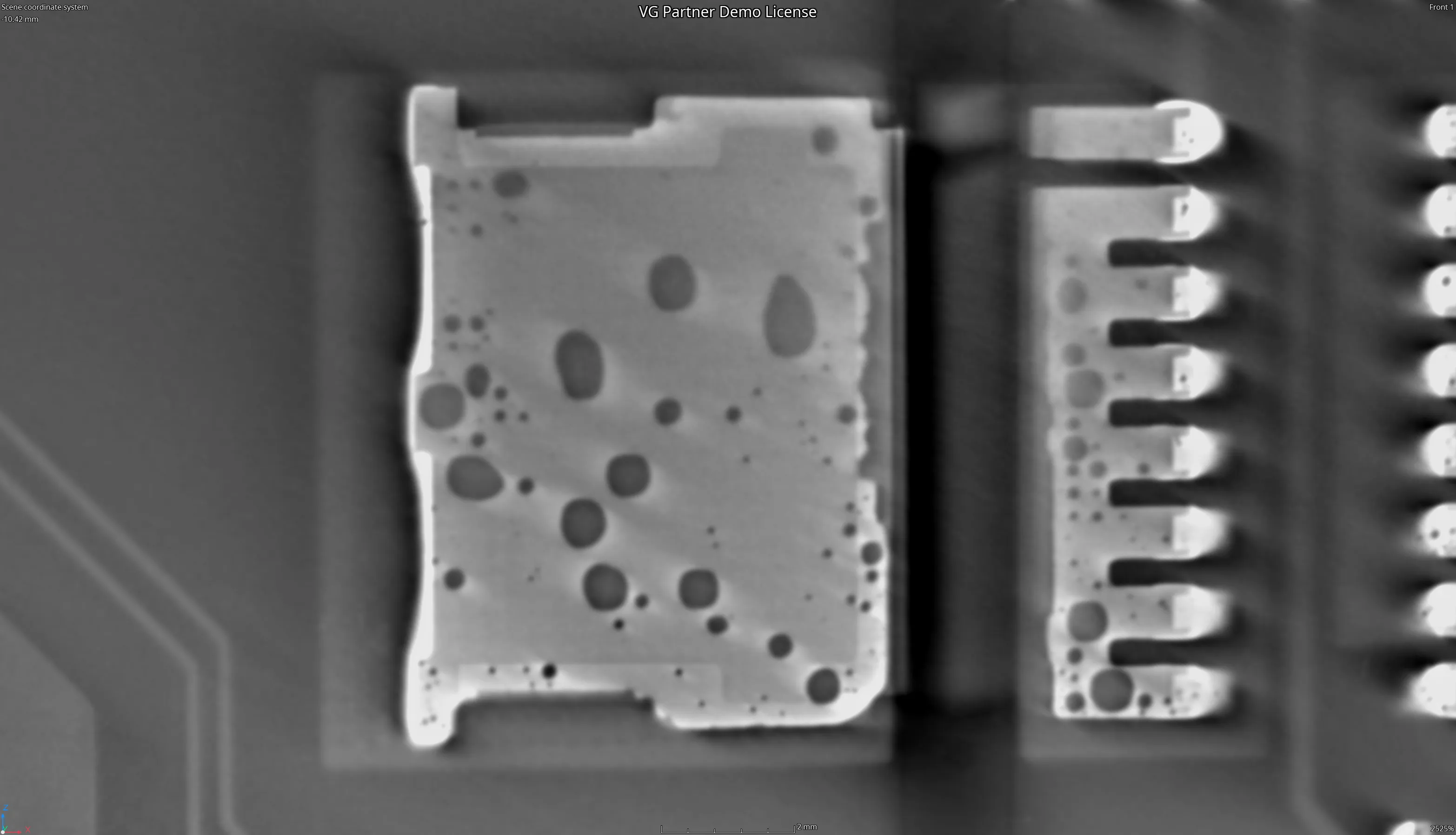
Power electronics for the data-centre boom need X-ray eyes on every joint
Application note ·
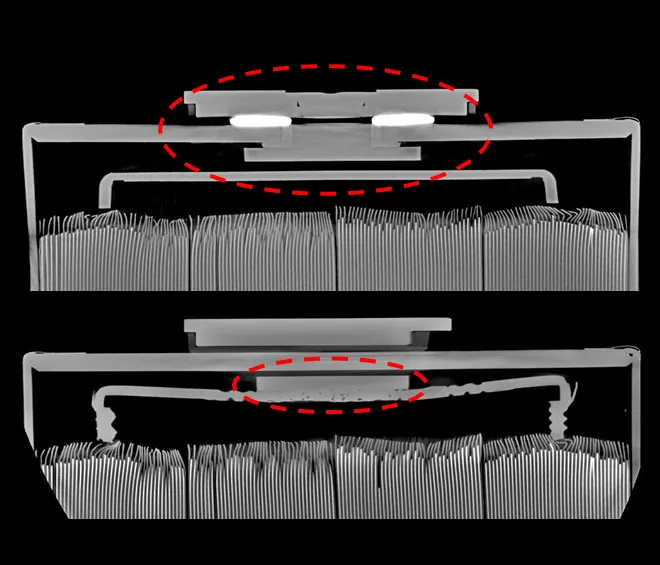
Module-level CT for gigafactory module and pack lines: glue coverage, busbars and cell position at line speed
Application note ·
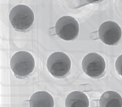
Sub-micron CT for advanced packaging: voids, micro-bumps and wire bonds in HBM and chiplet lines
Application note ·
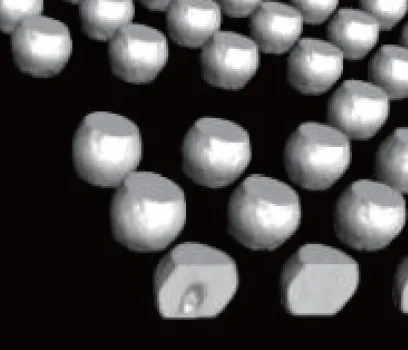
New semiconductor fabs and equipment plants need inspection designed in from day one
Application note ·