Application note ·
Sub-micron CT for advanced packaging: voids, micro-bumps and wire bonds in HBM and chiplet lines
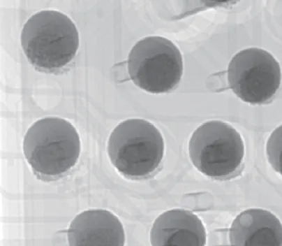
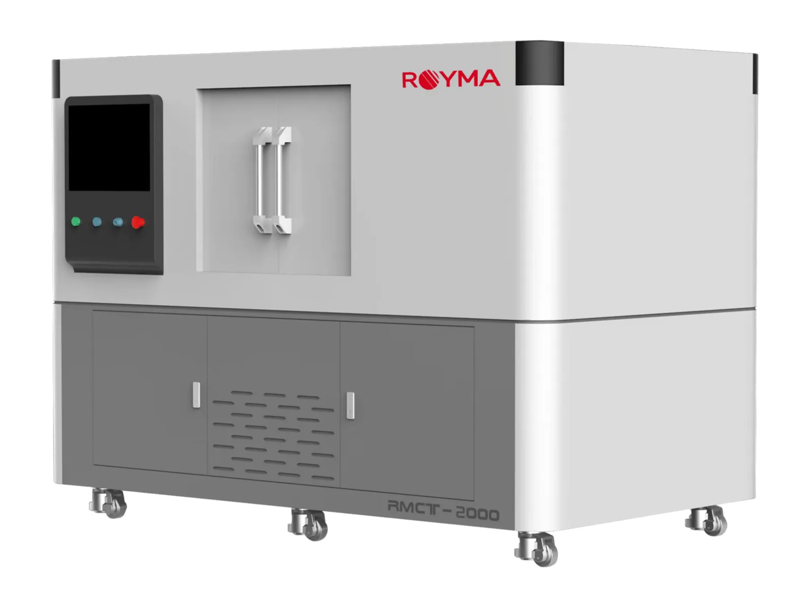
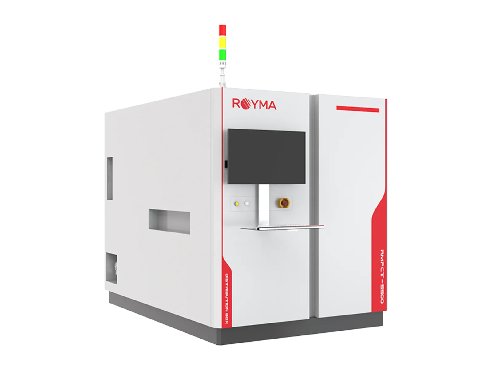
Royma Industrial CT inspects advanced packages at two scales. The RMCT2000HR nanofocus computed tomography (CT) machine resolves detail down to 0.5 µm for failure analysis. The RMPCT5500 planar CT checks package and board joints inline at up to 2 s per field of view.
The pairing is built for process and failure-analysis engineers working on stacked-die, chiplet and flip-chip packages. Both machines deliver 3D data without cutting the part open. A package that fails test keeps its evidence intact until you decide what to section.
3D CT separates what 2D X-ray superimposes
A stacked-die or chiplet package places dies, bumps and bond wires above one another within a few millimetres. A 2D X-ray image projects all of these layers into a single picture. A void in one bump layer and a harmless overlap with the layer below can then look the same.
Packaging capacity for high-bandwidth memory and chiplets is growing in Asia, North America and Europe. Every new line adds packages that need a non-destructive answer when they fail. Three inspection tasks recur:
- Failure analysis: locate the defect in a package that failed electrical test – which bump, which bond, which layer – before any cross-section is made.
- Process audit: check sampled packages and assembled boards for voids, bridging, head-in-pillow joints and misalignment.
- Inline control: verify the joints of flip-chip, PoP, LGA and CSP components at production rate.
Nanofocus CT resolves micro-voids and bonding defects
The RMCT2000HR is Royma’s laboratory CT for small, fine-structured samples. An open-tube nanofocus source runs from 110 to 190 kV. The machine reaches a 2D resolution down to 0.5 µm (JIMA) and a 3D resolution down to 1 µm.
It takes samples up to 150 × 150 × 150 mm and 5 kg. That covers single packages, dies, small modules and sections cut from larger boards. Measurement accuracy is stated as 3.0 + L/50 µm, L being the measured length.
At this scale the scan shows micro-porosity, micro-voids and micro-cracks, as well as inclusions and delamination between layers. Bond wires and chip-bonding interfaces appear in the same volume. You can step through the stack slice by slice and measure a void rather than describe it.
“A CT volume at this resolution shows which bump, which bond and which layer has failed,” says Gabor Szabo, Sales Director Europe at Royma Europe. “Your failure-analysis team sees the defect in place before deciding whether to cross-section.”
Planar CT brings 3D inspection onto the line
The RMPCT5500 uses planar CT, also called laminography, for flat parts that are too large for a rotating-sample scan. It switches between 2D, 2.5D and 3D planar CT and reconstructs more than 300 slices in the XY, XZ and YZ directions. Inspection time is up to 2 s per field of view.
Boards and substrates from 1 to 7 mm thick and up to 760 × 660 mm are handled directly. A laser-measured reference plane compensates up to ±2 mm of warp, so slices stay aligned to the joint level. The source runs from 40 to 180 kV, and resolution is selectable between 3 and 30 µm to match bump and ball size.
Royma’s application mapping for the RMPCT5500 includes flip-chip, PoP, LGA and CSP packages. The software quantifies the void ratio per solder land automatically. It also flags shorts, open joints, insufficient solder, ball shift and the pillow effect. The machine runs inline or at-line, with synchronous AOI and a connection to the plant’s MES.
Used together, the two machines form one inspection route. The RMPCT5500 checks every board or package at line rate and flags a suspect joint. That part then moves to the RMCT2000HR, where the defect is resolved at sub-micron scale without destroying it.
“Planar CT on the line and nanofocus CT in the lab look at the same package at two scales,” Szabo adds. “We scan your packages on both machines, so you compare real results before you choose a configuration.”
A test scan fixes the right configuration
The finest RMCT2000HR resolution is reached on small samples placed close to the source. Plan sample preparation around the 150 mm and 5 kg limit; full panels and assembled boards go to the RMPCT5500 instead. Because every package stack differs in materials and pitch, we recommend a test scan of your own parts before a configuration is fixed. More typical tasks are described on the semiconductor applications page.
| Stated figure | RMCT2000HR | RMPCT5500 |
|---|---|---|
| Role | Laboratory nanofocus CT | Inline or at-line planar CT |
| X-ray source | Open-tube nanofocus, 110–190 kV | 40–180 kV |
| Resolution | 2D down to 0.5 µm (JIMA); 3D down to 1 µm | Selectable, 3–30 µm |
| Sample size | Up to 150 × 150 × 150 mm | Up to 760 × 660 mm, 1–7 mm thick |
| Sample weight | Up to 5 kg | Up to 3.5 kg (optional 5 kg or 8 kg) |
| Imaging modes | 3D CT | 2D, 2.5D, 3D planar CT; more than 300 slices |
| Inspection time | – | Up to 2 s per field of view |
| Measurement accuracy | 3.0 + L/50 µm | – |
| Warp compensation | – | ±2 mm, laser-measured reference plane |
Royma Europe offers test scans of customer packages, dies and assembled boards on the RMCT2000HR and RMPCT5500. Contact Gabor Szabo, Sales Director Europe, Royma Europe, gabor_szabo@roymatek.eu, +49 15156503316 – www.roymatek.eu.
Royma Europe, Leibniz Universität Hannover – Institut für Produktentwicklung und Gerätebau, Gebäude 8143, An d. Universität 1, 30823 Garbsen, Germany.