Application note ·
Seeing inside advanced semiconductor packages before they leave the lab
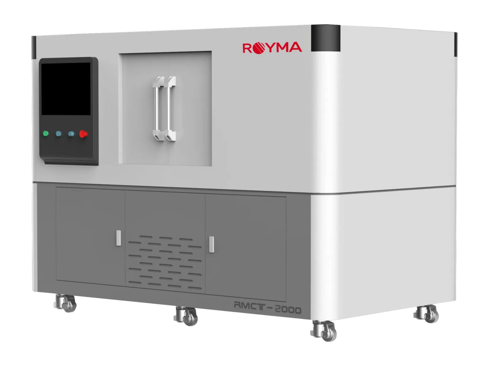
Royma Industrial CT gives semiconductor R&D and advanced-packaging labs a non-destructive 3D view inside finished packages. The RMCT2000 and RMCT2000HR nanofocus computed tomography (CT) machines separate stacked solder layers, bond wires and die attach without opening the part, with the RMCT2000HR resolving detail down to 0.5 µm in 2D.
This application note is written for process, qualification and failure-analysis engineers in semiconductor laboratories. It covers the inspection task, why 3D CT replaces a sharper 2D image, which machine suits which sample, and what a scan shows.
Laboratory CT keeps the evidence intact
New packaging and process-development labs are being built in North America, Europe and Asia. Their samples are few, often unique and expensive to replace. A package that fails electrical test or reliability stress still has to be analysed.
Cross-sectioning answers the question on one plane and destroys the sample. Decapsulation removes the mould compound and, with it, the original state of wires and joints. Laboratory CT answers first, in 3D, and leaves the package ready for electrical re-test, further stress or a targeted section.
3D CT separates what 2D X-ray superimposes
A ball grid array (BGA) places many rows of solder balls under one die. A package-on-package (PoP) stack adds a second device with its own joints directly above. In a 2D X-ray image all of these layers fall into one projection.
A void in the lower joint and a ball of the upper package can then look the same. So can a lifted bond wire and a wire crossing it at another height. The only non-destructive way to tell them apart is a reconstructed volume, sliced at the depth where each joint sits.
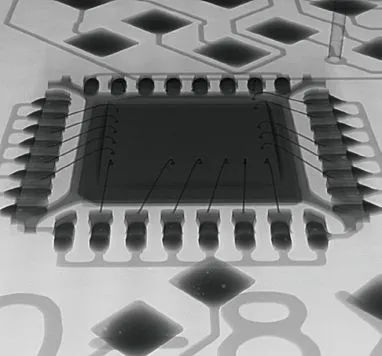
A CT volume can be viewed in the XY, YZ and XZ planes and stepped through layer by layer. Each solder joint, via, trace and bond wire is inspected in isolation from the layers above and below it.
The inspection task covers the whole package range
Royma’s laboratory CT is applied across the package types a development lab typically handles:
- Area-array and stacked packages: BGA and PoP, where joints hide behind other joints.
- Leaded and power packages: QFP, MOSFET and IGBT modules, with wire bonds, die attach and lead joints.
- LED packages and multilayer PCB assemblies, including vias and inner-layer traces.
The defects looked for are voids, bridging, non-wetting, cold joints and missing or insufficient solder. Head-in-pillow and open joints, misalignment and die-attach voids appear in the same volume. On wire-bonded parts, the scan shows broken, lifted or shorted wires and deviations in wire pitch.
“A failure-analysis engineer cannot choose the layer the defect sits on,” says Gabor Szabo, Sales Director Europe at Royma Europe. “With 3D CT you find the defect first and then decide where, or whether, to cut.”
Nanofocus CT resolves the finest interconnects
The RMCT2000 and RMCT2000HR are Royma’s laboratory CT machines for small, fine-structured samples. Both use an open-tube nanofocus X-ray source running from 110 to 190 kV.
The two versions differ in resolution. The RMCT2000HR reaches 0.5 µm in 2D (JIMA) and 1 µm in 3D. That is the scale of fine wire bonds, micro-bumps and micro-voids in die attach. The RMCT2000 reaches 2.5 µm in 2D and 3 µm in 3D, enough for routine joint checks on larger packages and board sections.
Both machines take samples up to 150 × 150 × 150 mm and 5 kg. That covers single packages, dies, power modules and sections cut from assembled boards. Measurement accuracy is stated as 3.0 + L/50 µm, L being the measured length.
Beyond solder joints: assembly and seal checks
The same scan answers questions that otherwise need disassembly. It shows seal integrity and connection quality inside encapsulated assemblies. It finds foreign particles and missing, misplaced or damaged fasteners in compact electronic devices. In connectors, it verifies pin alignment and contact integrity.
Hidden cracks in boards and components also show up in the volume. Because nothing is opened, the sample can be returned to test, kept as a reference or archived intact.
“Development labs often have one sample of a new package, not fifty,” Szabo adds. “A CT scan lets your team look inside it and still keep it for the next test.”
Practical notes for sample preparation
The finest RMCT2000HR resolution is reached on small samples placed close to the source. Plan sample size around the detail you need: the voxel size grows with the field of view. Where both overview and detail matter, scan the complete package on the RMCT2000 first, then a small region on the RMCT2000HR.
Fix samples firmly so they do not move during a long scan. Dense heat spreaders and thick copper reduce contrast in nearby joints, so orient the part to keep them out of the critical path where possible. Materials, pitch and stack height differ from package to package, so we recommend a test scan of your own parts before a configuration is fixed. More inspection tasks are described on the semiconductor applications page.
| Stated figure | RMCT2000 | RMCT2000HR |
|---|---|---|
| Role | Laboratory nanofocus CT | Laboratory nanofocus CT |
| X-ray source | Open-tube nanofocus, 110–190 kV | Open-tube nanofocus, 110–190 kV |
| 2D resolution | 2.5 µm | 0.5 µm (JIMA) |
| 3D resolution | 3 µm | 1 µm |
| Sample size | Up to 150 × 150 × 150 mm | Up to 150 × 150 × 150 mm |
| Sample weight | Up to 5 kg | Up to 5 kg |
| Measurement accuracy | 3.0 + L/50 µm | 3.0 + L/50 µm |
| Detector | CsI, 3072 × 3072 pixels | CsI, 3072 × 3072 pixels |
Test scans of your packages
Royma Europe offers test scans of customer packages, dies and board sections on the RMCT2000 and RMCT2000HR, with an evaluation of the defects and resolution reached on your own parts.
Contact: Gabor Szabo, Sales Director Europe, Royma Europe – gabor_szabo@roymatek.eu – +49 15156503316 – www.roymatek.eu
Royma Europe, Leibniz Universität Hannover – Institut für Produktentwicklung und Gerätebau, Gebäude 8143, An d. Universität 1, 30823 Garbsen, Germany.