
Application note ·
New semiconductor fabs and equipment plants need inspection designed in from day one
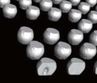
Royma Industrial CT helps new semiconductor and equipment plants plan non-destructive 3D inspection into their lines from the start. Inline CT makes automated pass/fail decisions on solder joints on the line, and Laboratory CT resolves stacked and encapsulated interconnects for failure analysis. Both work under a quality system certified to ISO 9001:2015.
This application note is for quality and industrialisation engineers qualifying a new site, line or product. It shows which tasks computed tomography (CT) takes on and which machine class suits each.
Inspection planned at line design shortens qualification
New wafer-fab, cleanroom and equipment-manufacturing capacity is being built across Europe. Every new line has to prove to its customers that the parts it ships are sound, and much of that proof depends on joints nobody can see.
Power modules, control boards and sensor assemblies hide their critical connections under packages, heat spreaders and other layers. When inspection is added after the line is running, it tends to arrive as a manual 2D X-ray station and a queue of cross-sections. When it is planned with the line, the inspection points, data records and acceptance criteria are part of qualification from the first lot.
Three tasks recur on new electronics and equipment lines:
- Production control: an objective pass/fail decision on every solder joint that matters, with a record per part.
- Process set-up: measuring solder voids in hidden BGA and thermal-pad joints while reflow profiles are tuned.
- Failure analysis: locating the defect in a returned or failed part without destroying the evidence.
Inline CT turns solder inspection into a production step
Royma Inline CT automates X-ray and CT solder inspection in 2D and 3D. The machine gives a repeatable Go/NoGo decision per part and keeps a traceable record of each decision. That replaces operator judgement on grey-scale images with the same criterion on every shift.
In 3D, Inline CT quantifies solder-void volume and distribution, including joints hidden under BGA packages and thermal pads. This is where 2D X-ray struggles: a void in one layer and a pad in the layer below project onto the same spot. With a void volume per joint, your process engineers can tie a reflow setting to a measured result rather than to an impression.
The defects addressed on the line are voids, bridges, insufficient fill and misaligned connections.
“A new line has no inspection history, so every decision has to be documented from the first lot,” says Gabor Szabo, Sales Director Europe at Royma Europe. “Inline CT gives your team an automatic pass/fail and a record that a customer auditor can follow.”
Laboratory CT separates what 2D X-ray superimposes
A package that fails electrical test, a returned power module or a first-article board needs a closer look than line rate allows. Royma Laboratory CT scans the part in 3D and separates overlapping and stacked solder and interconnect layers without decapsulation or cross-sectioning.
The engineer views the volume along the XY, YZ and XZ planes and steps through a multilayer board layer by layer. Solder joints, vias, traces and bond wires appear in the same data set. The scan covers BGA, PoP and QFP packages, MOSFET and IGBT power devices, LEDs and multilayer printed circuit boards.
At this level the data shows voids, bridging, non-wetting, cold joints and missing or insufficient solder. It also shows head-in-pillow and open joints, wire-bond breaks, lifts, shorts and pitch deviation, die-attach voids and package misalignment. The part stays intact, so you decide afterwards whether a cross-section is still needed and where to make it.
Used together, the two machine classes form one route. Inline CT flags a suspect joint on the line; the part then moves to Laboratory CT, where the cause is found in 3D.
Certified quality and early criteria support qualification
Inspection equipment is itself part of a new plant’s quality system and passes through the same procurement gates. Royma works under a quality management system certified to ISO 9001:2015, with environmental management to ISO 14001:2015 and occupational health and safety to ISO 45001:2018. Royma also holds CE and UL certification, and third-party test reports cover dimensional measurement, resolution and penetration.
| Stated item | What is stated |
|---|---|
| Quality management | ISO 9001:2015 |
| Environmental management | ISO 14001:2015 |
| Occupational health and safety | ISO 45001:2018 |
| Product conformity | CE and UL certification |
| Inline CT | Automated 2D/3D solder inspection; Go/NoGo decision with full traceability; 3D solder-void volume and distribution, including hidden BGA and thermal-pad joints |
| Laboratory CT | 3D separation of stacked solder and interconnect layers; XY, YZ and XZ views; layer-by-layer inspection without disassembly |
| Package types covered | BGA, PoP, QFP, MOSFET, IGBT, LED, multilayer PCB |
Fix the inspection points and the acceptance criteria for each critical joint while the line layout is still open; a CT station needs its place in the material flow. Void acceptance limits depend on the package, the pad design and your customer’s requirement, so we recommend setting them on scans of your own parts. More typical tasks are described on the semiconductor applications page.
“The best time to agree an inspection concept is before the first machine is ordered,” Szabo adds. “We scan your parts and help you set the criteria your line will be qualified against.”
Royma Europe offers test scans of customer packages, power modules and assembled boards on Inline CT and Laboratory CT, and support in defining inspection points for a new line. Contact Gabor Szabo, Sales Director Europe, Royma Europe, gabor_szabo@roymatek.eu, +49 15156503316 – www.roymatek.eu.
Royma Europe, Leibniz Universität Hannover – Institut für Produktentwicklung und Gerätebau, Gebäude 8143, An d. Universität 1, 30823 Garbsen, Germany.