
Application note ·
Power electronics for the data-centre boom need X-ray eyes on every joint
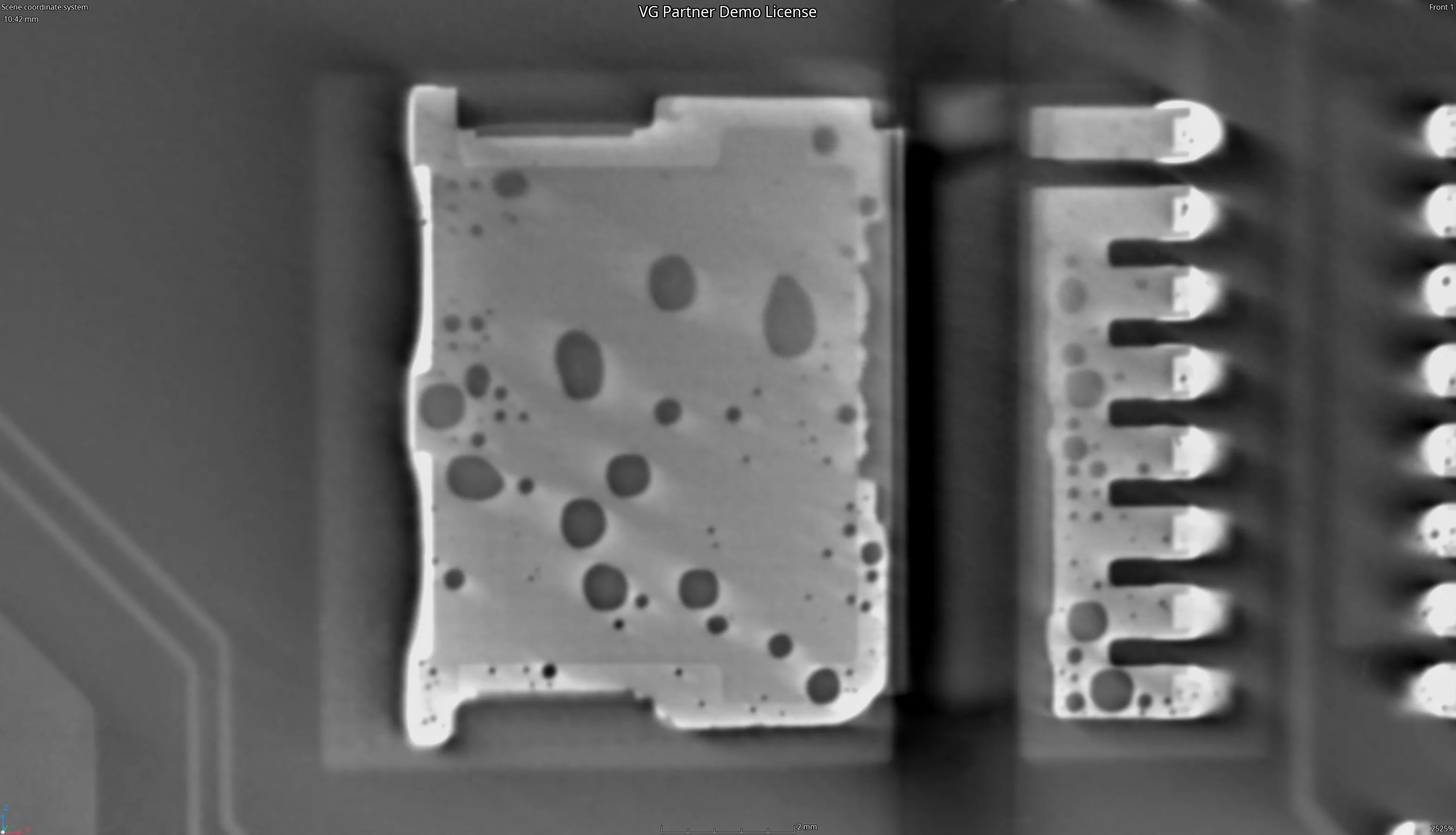
Royma Industrial CT offers automated inline CT for power-electronics production. It inspects solder joints and interconnects in 2D and 3D and returns a pass/fail decision with a traceable record for every part. For failure analysis, Royma laboratory CT resolves the same joints layer by layer without cutting the assembly open.
The combination is built for quality and manufacturing engineers who produce power modules, converters and control boards for mission-critical use. Data-centre power supply is one of these fields. Demand for power hardware in data centres is rising in North America, Europe and Asia, and production lines are growing with it.
Inline CT turns solder inspection into a pass/fail step
Power electronics concentrate current in a small number of large joints. A void under a thermal pad or a die attach reduces the area that carries heat away. A 2D X-ray image projects every layer of the assembly into one picture, so these voids are hard to separate from the structures above and below them.
Royma Inline CT inspects solder joints automatically in 2D and 3D. Every part receives a Go/NoGo decision against your acceptance criteria. The decision is repeatable and does not depend on an operator’s judgement at the end of a shift.
The 3D data quantifies solder voids by volume and by distribution. This includes joints hidden under components, such as ball grid arrays (BGA) and thermal pads. The machine detects:
- voids and void distribution in solder layers and thermal pads
- bridges between neighbouring joints
- insufficient solder fill and missing solder
- misaligned connections and components
Each result is stored with the part. When a customer asks about a delivered unit, you retrieve its inspection record instead of reconstructing the history from samples.
“Power modules for data centres run continuously, so a hidden void matters,” says Gabor Szabo, Sales Director Europe at Royma Europe. “Inline CT gives every part a recorded pass/fail decision, not just the parts you happened to sample.”
Laboratory CT separates stacked layers for failure analysis
When a part fails electrical test or a line flags a trend, the question is which joint failed and why. Royma Laboratory CT answers it non-destructively. The computed tomography (CT) volume separates overlapping and stacked solder and interconnect layers without decapsulation or cross-sectioning.
You view the part in XY, YZ and XZ slices and step through a multilayer board layer by layer. Solder joints, vias, traces and bond wires appear in the same volume. The evidence stays intact until you decide whether to section.
Royma laboratory CT covers the package types found in power and control electronics. These include MOSFET and IGBT power devices, BGA, package-on-package (PoP), QFP and LED packages, and multilayer printed circuit boards. Typical findings are:
- voids, non-wetting and cold joints
- head-in-pillow and open joints
- wire-bond breaks, lift-off, shorts and pitch deviation
- die-attach voids and package-level misalignment
One inspection route from line to lab
Used together, the two machine classes form one route. Inline CT checks every part at the line and flags a suspect joint. That part moves to laboratory CT, where the defect is resolved in 3D and the root cause is traced back to the reflow or assembly process.
Consistent 3D void data also supports process control. Void volume per joint gives an objective measure of reflow quality. Trends become visible before they turn into rejects.
Royma’s software chain covers acquisition, 3D reconstruction, visualisation and analysis, and database management. AI-assisted defect recognition is part of this chain and is being developed further for electronics inspection. The analysis settings are agreed with you for your parts and acceptance criteria.
“We start with your own boards and modules,” Szabo adds. “A test scan shows which defects inline CT decides automatically and which ones go to the lab.”
Stated capabilities at a glance
| Inspection task | Royma machine class | What the data shows |
|---|---|---|
| Automated solder inspection | Inline CT | Go/NoGo decision per part in 2D and 3D, with full traceability |
| Solder-void quantification | Inline CT | Void volume and distribution, including hidden BGA and thermal-pad joints |
| Defect detection at the line | Inline CT | Voids, bridges, insufficient fill, misaligned connections |
| Layer separation | Laboratory CT | Overlapping and stacked solder and interconnect layers, without decapsulation or cross-sectioning |
| Board inspection | Laboratory CT | Solder joints, vias, traces and bond wires, layer by layer, in XY, YZ and XZ views |
| Package coverage | Laboratory CT | MOSFET, IGBT, BGA, PoP, QFP, LED packages and multilayer boards |
A test scan fixes the configuration
Power modules differ in size, materials and joint design. Cycle time, resolution and part handling depend on these factors, so we recommend a test scan of your own parts before a configuration is fixed. The scan shows which defects the inline decision covers and which call for laboratory analysis. More typical tasks are described on the data-centre applications page and the consumer electronics applications page.
Royma Europe offers test scans and evaluation of customer power modules, converters and assembled boards. Contact Gabor Szabo, Sales Director Europe, Royma Europe, gabor_szabo@roymatek.eu, +49 15156503316 – www.roymatek.eu.
Royma Europe, Leibniz Universität Hannover – Institut für Produktentwicklung und Gerätebau, Gebäude 8143, An d. Universität 1, 30823 Garbsen, Germany.