
Application note ·
Royma Laboratory CT measures IGBT solder voids and die-attach voids in power modules
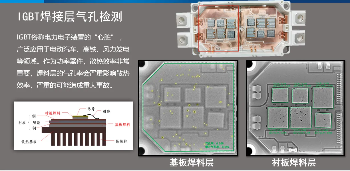
Royma Laboratory CT measures IGBT solder voids and die-attach voids in power modules layer by layer. The computed tomography (CT) scan separates the substrate solder layer and the baseplate solder layer of an IGBT or MOSFET module in 3D and shows the voids of each layer on their own – without decapsulation and without cross-sectioning.
Royma’s Laboratory CT systems scan the complete module as delivered and return one volume data set. From that data set, the inspection covers:
- Layer separation: die attach, substrate solder and baseplate solder viewed as separate slices instead of one superimposed image.
- Multi-axis viewing: XY, YZ and XZ sections through any point of the module.
- Solder defects: voids, non-wetting and missing or insufficient solder, located in the layer where they sit.
- Interconnects: bond wires checked for breaks, lift-off, shorts and pitch deviation in the same scan.
Each solder layer as its own result
An IGBT or MOSFET power module conducts heat from the chip through the die attach, a ceramic substrate and a second, larger solder layer into the baseplate. A void in either solder layer interrupts that heat path at the point where it sits. A 2D X-ray image projects both layers onto one plane, so a void under a chip and a void under the substrate appear in the same picture and cannot be assigned to a layer.
Royma Laboratory CT reconstructs the module as a volume and places a slice exactly in the plane of each solder layer. The substrate solder and the baseplate solder become two separate images, each with its own void picture. The engineer sees which layer carries a void, where it lies relative to the chips above it, and whether it is a single large void or a field of small ones.
“With 3D CT the two solder layers of a power module stop being one image,” says Gabor Szabo, Sales Director Europe, Royma Europe. “You see the die attach under every chip and the full baseplate solder as separate results, and you can trace each void to the layer and the process step that produced it.”
Die-attach voids under every chip
The die attach is the first thermal interface below each IGBT, MOSFET or diode chip. Royma Laboratory CT shows the solder area under every chip of the module in one scan, with voids marked inside the chip outline. Voids at the edge of the chip, voids in the centre and areas of non-wetting are distinguished in the slice, because each appears at its true position rather than overlaid by the substrate solder below.
Sections in the YZ and XZ planes add the third dimension. They show whether a void runs through the full height of the solder layer or sits at one interface, and they show tilt or uneven thickness of the solder under a chip. This is the view a failure analysis otherwise obtains by grinding a cross-section through one chip – the CT scan provides it for every chip, and the module stays intact.
Baseplate solder across the full substrate area
The baseplate solder is the largest solder area in the module and carries the heat of all chips into the cooling path. Royma Laboratory CT renders this layer as one slice over the full substrate area. Voids are visible as a map: their distribution, their position under or between the chip sites, and larger voids at the substrate edge where solder flow ends.
Because the slice is taken in the baseplate solder plane only, the chips, bond wires and terminals above it no longer cover the void picture. The same data set then gives the die-attach slice and the baseplate slice of the same module, so the two layers can be compared directly for one part.
Bond wires and interconnects in the same data set
The scan that shows the solder layers also contains the interconnects. Royma Laboratory CT inspects bond wires for breaks, lift-off at the bond foot, shorts between neighbouring wires and pitch deviation, and shows the terminals and their joints to the substrate. Package-level misalignment, such as a shifted substrate or chip, is visible in the same volume.
“A single scan answers the solder question and the interconnect question for the same module,” adds Szabo. “That keeps the part available for further testing after the inspection.”
Inspection without decapsulation
The module is scanned closed, with its housing and gel in place. The scan is non-destructive, so the same module can go on to electrical or thermal testing afterwards, or be scanned again after testing to compare the void picture before and after. Royma Laboratory CT supports both routine sampling of production lots and the analysis of single returned or failed modules.
The detail visible in a scan depends on module size, the materials in the beam path and the scan set-up. Royma therefore confirms the achievable void detection on a test scan of the customer’s own module before recommending a configuration. The method suits power modules for automotive drives and the wider semiconductor packaging range, including discrete MOSFET packages.
| Inspection task | What Royma Laboratory CT shows |
|---|---|
| Die attach | Voids and non-wetting under each chip, in the chip outline |
| Substrate and baseplate solder | Void map over the full area, separated by layer |
| Solder geometry | Tilt and uneven thickness in YZ and XZ sections |
| Bond wires | Breaks, lift-off, shorts, pitch deviation |
| Assembly | Misalignment of chips and substrates |
Test scans available
Royma Europe offers test scans of IGBT and MOSFET power modules on its Laboratory CT systems, together with inspection services for single modules and lots. Contact Gabor Szabo, Sales Director Europe, Royma Europe, gabor_szabo@roymatek.eu, +49 15156503316 – www.roymatek.eu.
Royma Europe, Leibniz Universität Hannover – Institut für Produktentwicklung und Gerätebau, Gebäude 8143, An d. Universität 1, 30823 Garbsen, Germany.
About Royma: Royma Industrial CT develops and builds industrial X-ray and computed tomography systems, from 2D X-ray to horizontal, gantry, planar and inline CT.