News ·
Non-destructive stub and via verification for backplane and power-electronics board production
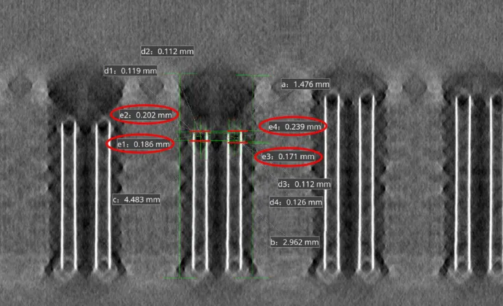
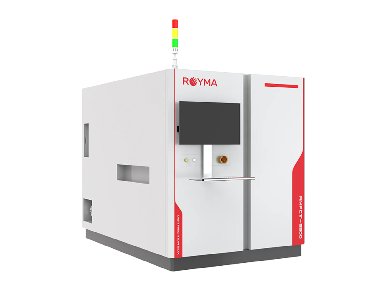
The RMPCT5500 planar computed tomography (CT) machine from Royma Industrial CT verifies back-drilled stubs and vias without cutting the board. One full-field 3D scan measures stub depth, residual copper height, layer spacing and hole eccentricity. Each pad receives an automatic pass or fail result that goes straight to your MES.
The function is built for quality and process engineers in EMS and power-electronics production. It covers multilayer printed circuit boards, backplanes and IGBT substrates. You check the boards you ship, not a sample that ends up in the scrap bin.
Non-destructive measurement replaces the cross-section
Back-drilling removes the unused part of a plated via. What remains must sit within tolerance. A stub that is too long disturbs high-speed signals. A drill that goes too deep damages the connection it should protect.
The established check is metallurgical cross-sectioning. A sample board is cut, polished and examined under a microscope. The result is valid for one plane of one board, and the board is lost. The method is destructive, single-angle and slow.
The RMPCT5500 replaces that step with a non-destructive full-field 3D tomographic scan. The board stays intact and can go back into the line. You can scan the same board again after rework and compare the results.
“Our customers want the certainty of a cross-section without cutting the board,” says Gabor Szabo, Sales Director Europe at Royma Europe. “The CT scan gives them that answer for the board they actually deliver.”
One scan measures four via features
The RMPCT5500 reconstructs the board volume rather than a single sectioned plane. From that one scan, the software measures four features at each back-drilled via:
- back-drilled stub depth
- residual copper height
- layer spacing
- hole and via eccentricity
Because the whole volume is available, the measurement is repeatable and can be viewed from several angles. A cross-section shows one cut. The CT volume shows every via in the scanned field.
This matters most in high-mix production. Backplanes, multilayer boards and IGBT substrates differ in layer count, drill pattern and material. The same scan-and-measure routine applies to each of them once the limits are set.
Automatic pass/fail per pad, exported to MES
You set upper and lower limits for each measured feature. The software compares every measurement against those limits and flags each pad as OK or NG. The operator reads a verdict, not a slice image that needs interpretation.
The results are exportable for MES and data traceability. Each finding stays tied to the board and the pad where it was measured. When a customer asks about a delivered board, you retrieve its record instead of a sampling report.
The same data supports process control. Drift in drill depth or residual copper becomes visible across boards and lots. You can correct the drilling process before the drift turns into rejects.
“The line gets a measured value and a verdict for every via, not a scrapped sample,” Szabo adds. “That changes stub verification from an audit into part of production.”
Growing board production needs a faster check
EMS and power-electronics plants in Europe, Asia and North America are expanding production of multilayer boards, backplanes and power substrates. More boards and more vias per board increase the load on a sampling-based cross-section lab. A non-destructive, automated check scales with the line instead.
The RMPCT5500 combines this stub and via measurement with its other planar CT inspection tasks on the same machine. The back-drill analysis is described in more detail in our application note on inline 3D planar CT for HDI boards. Further electronics inspection tasks are on the consumer electronics application page.
Measurement settings depend on board thickness, via size and the features you need. We recommend a test scan of your own boards before a configuration is fixed.
Test scans of your boards
Royma Europe offers test scans and evaluation of customer boards, backplanes and substrates on the RMPCT5500. Send us a board with back-drilled vias and your tolerance limits, and we show you the measured result per pad.
Contact Gabor Szabo, Sales Director Europe, Royma Europe, gabor_szabo@roymatek.eu, +49 15156503316 – www.roymatek.eu.
Royma Europe, Leibniz Universität Hannover – Institut für Produktentwicklung und Gerätebau, Gebäude 8143, An d. Universität 1, 30823 Garbsen, Germany.